
Keszoox
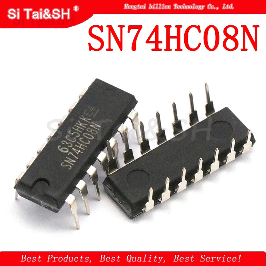
SN74HC08N Quad 2-Input AND Gate Logic IC DIP-14 – Pack of 5 (74HC08)
SN74HC08N Quad 2-Input AND Gate Logic IC DIP-14 – Pack of 5 (74HC08)

Couldn't load pickup availability
SN74HC08N (74HC08) Quad 2-Input AND Gate — DIP-14, 2–6V, 25mA (5-Pack)
The SN74HC08N contains four independent 2-input AND gates in a DIP-14 through-hole package, operating from 2V to 6V with CMOS logic levels. The AND gate output is HIGH only when both inputs are HIGH, making it the fundamental building block for signal gating, clock enable circuits, combinational logic, and digital control systems. With 25mA output drive and 7ns propagation delay at 5V, it is suitable for both low-speed control logic and higher-frequency digital circuits.
Key Specifications
| Parameter | Value |
|---|---|
| Package | DIP-14 (through-hole) |
| Gates | 4× 2-input AND |
| Logic Family | 74HC (High-Speed CMOS) |
| Supply Voltage | 2V – 6V |
| Input Logic Levels | VIH ≥ 70% VCC, VIL ≤ 30% VCC |
| Output Drive Current | ±25mA per output |
| Propagation Delay | ~7ns (VCC=5V) |
| Operating Temperature | -40°C to +125°C |
| Quantity | 5 pieces |
AND Gate Truth Table
| Input A | Input B | Output Y |
|---|---|---|
| 0 | 0 | 0 |
| 0 | 1 | 0 |
| 1 | 0 | 0 |
| 1 | 1 | 1 |
74HC08 vs 74HC00 (NAND) vs 74HC32 (OR)
| IC | Function | Output HIGH when | Common Use |
|---|---|---|---|
| 74HC08 (AND) | A AND B | Both inputs HIGH | Signal gating, clock enable |
| 74HC00 (NAND) | NOT(A AND B) | Any input LOW | Universal gate, SR latch |
| 74HC32 (OR) | A OR B | Any input HIGH | Signal combining, interrupt OR |
| 74HC86 (XOR) | A XOR B | Inputs differ | Parity, comparator |
Why Choose SN74HC08N?
- AND gate function — output HIGH only when both inputs HIGH, ideal for conditional signal gating
- 2–6V supply — compatible with 3.3V (ESP32, STM32) and 5V (Arduino) systems
- 25mA output drive — directly drives LEDs, logic inputs, and small loads
- 4 gates per IC — four independent AND gates in one DIP-14 package
- 5-pack value — sufficient for multiple logic circuit builds and experiments
Compatible With / Common Use Cases
- Clock enable gate: AND gate between clock signal and enable pin — clock passes only when enable is HIGH
- Signal gating: Gate a data signal with a control signal — data passes only when control is HIGH
- Interrupt masking: AND interrupt signal with mask bit to selectively enable/disable interrupts
- Combinational logic: Implement complex Boolean expressions using AND gates with other logic ICs
- Digital electronics education: Breadboard AND gate experiments for Boolean algebra and logic design
Frequently Asked Questions
Q: How do I use 74HC08 as a clock enable circuit?
A: Connect the clock signal to input A of one AND gate. Connect the enable signal (from MCU GPIO or control logic) to input B. The output delivers the clock signal only when enable is HIGH. When enable is LOW, output stays LOW regardless of clock state. This prevents spurious clock edges when enabling/disabling a clock domain.
Q: Can I use 74HC08 with 3.3V Arduino or ESP32?
A: Yes — 74HC08 operates from 2V to 6V. At 3.3V supply, VIH = 70% × 3.3V = 2.31V and VIL = 30% × 3.3V = 0.99V. ESP32 GPIO outputs 3.3V HIGH and 0V LOW, which meets these thresholds. The output at 3.3V supply is also 3.3V logic, compatible with other 3.3V devices.
Q: What is the difference between 74HC08 and 74HCT08?
A: 74HC08 has CMOS input thresholds (VIH = 70% VCC). 74HCT08 has TTL-compatible input thresholds (VIH = 2.0V fixed), making it compatible with 5V TTL outputs while providing CMOS output levels. Use 74HCT08 when interfacing with 74LS or other TTL logic families. For pure CMOS systems (Arduino, ESP32, STM32), 74HC08 is the correct choice.
Package Contents
- 5× SN74HC08N (74HC08) Quad 2-Input AND Gate IC (DIP-14)