
Keszoox
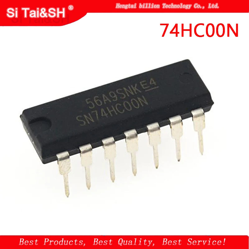
74HC00N Quad 2-Input NAND Gate — DIP-14 Through-Hole, 2–6V, -40°C to 125°C (5-Pack)
74HC00N Quad 2-Input NAND Gate DIP-14 Through-Hole, 2–6V, -40°C to 125°C (5-Pack)

Couldn't load pickup availability
74HC00N / SN74HC00N Quad 2-Input NAND Gate — DIP-14, 2–6V, -40°C to +125°C (5-Pack)
The 74HC00N (SN74HC00N) contains four independent 2-input NAND gates in a DIP-14 through-hole package, operating from 2V to 6V with CMOS logic levels. As the universal logic gate (any Boolean function can be implemented using only NAND gates), it is the most fundamental building block in digital logic design. With 25mA output drive, 100MHz+ switching speed, and -40°C to +125°C operating range, it is used in combinational logic circuits, oscillators, inverters, and digital electronics education.
Key Specifications
| Parameter | Value |
|---|---|
| Package | DIP-14 (through-hole) |
| Gates | 4× 2-input NAND |
| Logic Family | 74HC (High-Speed CMOS) |
| Supply Voltage | 2V – 6V |
| Input Logic Levels | VIH ≥ 70% VCC, VIL ≤ 30% VCC (CMOS) |
| Output Drive Current | ±25mA per output |
| Propagation Delay | ~7ns (VCC=5V) |
| Max Clock Frequency | >100MHz |
| Operating Temperature | -40°C to +125°C |
| Quantity | 5 pieces |
74HC00 NAND Gate Truth Table
| Input A | Input B | Output Y |
|---|---|---|
| 0 | 0 | 1 |
| 0 | 1 | 1 |
| 1 | 0 | 1 |
| 1 | 1 | 0 |
74HC00 vs 74LS00 vs 74HCT00
| Feature | 74HC00 (CMOS) | 74LS00 (TTL) | 74HCT00 (CMOS/TTL) |
|---|---|---|---|
| Supply Voltage | 2–6V | 5V only | 4.5–5.5V |
| Input Levels | CMOS (70% VCC) | TTL (VIH=2.0V) | TTL (VIH=2.0V) |
| Power consumption | Very low (CMOS) | Higher (TTL) | Very low (CMOS) |
| Speed | ~7ns | ~10ns | ~7ns |
| Best for | New CMOS designs, 3.3V/5V | Legacy TTL repair | TTL-to-CMOS interface |
Why Choose 74HC00N?
- Universal gate — any logic function (AND, OR, NOT, XOR, flip-flop) can be built from NAND gates alone
- 2–6V supply — works with 3.3V (ESP32, STM32) and 5V (Arduino) systems
- 25mA output drive — directly drives LEDs, small loads, and other logic inputs
- 100MHz+ speed — suitable for high-frequency oscillator and clock generation circuits
- 5-pack value — sufficient for multiple logic circuit builds and experiments
Compatible With / Common Use Cases
- Logic inverter: Tie both inputs together — NAND with both inputs = NOT gate (inverter)
- NAND oscillator: RC oscillator using two NAND gates as inverters for clock generation
- SR latch: Two cross-coupled NAND gates form a Set-Reset latch (basic memory element)
- Combinational logic: Implement AND, OR, XOR using NAND gate combinations
- Digital electronics education: Breadboard logic circuit experiments for Boolean algebra and digital design
Frequently Asked Questions
Q: How do I make an inverter (NOT gate) from 74HC00N?
A: Connect both inputs of one NAND gate together. When both inputs are HIGH (1,1), output is LOW (NAND truth table: 1,1→0). When both inputs are LOW (0,0), output is HIGH (0,0→1). This gives NOT gate behavior: output = NOT(input). Each 74HC00N provides 4 inverters this way.
Q: How do I build an SR latch from 74HC00N?
A: Use two NAND gates cross-coupled: Gate 1 output connects to Gate 2 input B; Gate 2 output connects to Gate 1 input B. Gate 1 input A = ̅S̅ (active-low Set), Gate 2 input A = ̅R̅ (active-low Reset). Gate 1 output = Q, Gate 2 output = ̅Q̅. Pull ̅S̅ LOW to Set (Q=1), pull ̅R̅ LOW to Reset (Q=0). Both HIGH = hold state.
Q: Can 74HC00N drive an LED directly?
A: Yes — 74HC00N output can sink or source 25mA. For a 5V supply and red LED (VF=2.0V, IF=10mA): R = (5 − 2.0) / 0.010 = 300Ω. Use 330Ω standard value. Connect LED anode to 5V, cathode through 330Ω to NAND output (active-low drive: LED on when output LOW). For active-high drive, connect LED anode to NAND output through 330Ω, cathode to GND.
Package Contents
- 5× 74HC00N / SN74HC00N Quad 2-Input NAND Gate IC (DIP-14)