

Keszoox
Double-Sided Prototype PCB Board — Universal Printed Circuit Board for DIY Electronics
Double-Sided Prototype PCB Board Universal Printed Circuit Board for DIY Electronics

Couldn't load pickup availability
Double-Sided Prototype PCB Board — Universal Printed Circuit Board for DIY Electronics
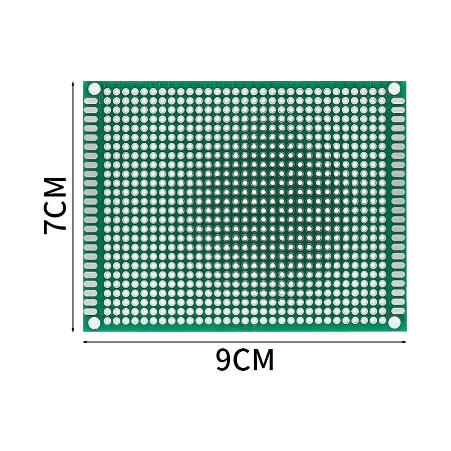
These double-sided prototype PCB boards provide a durable, professional-grade platform for building and testing electronic circuits without the lead time and cost of custom PCB fabrication. Made from FR4 fiberglass with a standard 2.54mm (0.1″) pitch hole grid, they accept through-hole components, DIP ICs, pin headers, and terminal blocks directly. The double-sided copper layer allows routing on both sides for more complex circuit layouts.
Key Specifications
| Parameter | Value |
|---|---|
| Material | FR4 fiberglass (1.6mm thickness) |
| Copper Layers | Double-sided (top + bottom copper) |
| Hole Pitch | 2.54mm (0.1″) standard grid |
| Hole Diameter | 1.0mm (standard through-hole) |
| Surface Finish | HASL (Hot Air Solder Leveling) or bare copper |
| Size Options | Multiple sizes available (select variant) |
| Compatible Components | DIP ICs, resistors, capacitors, pin headers, terminal blocks, transistors |
| Origin | CN |
Why Double-Sided vs Single-Sided?
- More routing options — Use the bottom copper layer for ground planes, power rails, or signal traces that would otherwise require jumper wires on a single-sided board
- Cleaner layouts — Reduce the number of point-to-point wire jumpers needed for complex circuits
- Better ground planes — Flood-fill the bottom layer as a ground plane to reduce noise in analog and RF circuits
- FR4 durability — Fiberglass substrate withstands repeated soldering and desoldering without warping or delaminating
Typical Applications
- Arduino and ESP32 shield and breakout board prototyping
- Analog circuit testing (op-amp, filter, amplifier designs)
- Power supply and voltage regulator circuit builds
- Sensor interface and signal conditioning circuits
- Educational electronics lab projects
- One-off custom PCB builds for enclosure mounting
Frequently Asked Questions
Q: Can I use this with SMD components?
These boards are designed for through-hole components with 2.54mm pitch. SMD components can be soldered to the copper pads with care, but the 2.54mm hole grid is not optimized for fine-pitch SMD work. For SMD prototyping, use a dedicated SMD prototype board with 0.5–1.27mm pitch pads.
Q: How do I connect traces between holes?
Use solder bridges between adjacent pads, 30AWG wire-wrap wire for longer connections, or copper tape for bus connections. For permanent builds, use rosin-core solder and flux for clean, reliable joints.
Package Contents
- Double-sided prototype PCB board(s) (size and quantity per selected variant)