

Keszoox
SG3525A SG3525ADR SOP-16 PWM Controller IC Chipset
SG3525A SG3525ADR SOP-16 PWM Controller IC Chipset

Couldn't load pickup availability
SG3525A / SG3525ADR SOP-16 PWM Controller IC — Switch-Mode Power Supply Driver
The SG3525A is one of the most widely deployed voltage-mode PWM controller ICs in power electronics, originally developed by Silicon General and now produced by multiple manufacturers including Texas Instruments, STMicroelectronics, and ON Semiconductor. Its push-pull complementary output stage directly drives two power switches (N-channel MOSFETs, IGBTs, or NPN BJTs) with programmable dead time — making it the go-to controller for half-bridge, full-bridge, and push-pull SMPS topologies from 100W to multi-kW.
The SG3525ADR is the same device in SOP-16 SMD package, suitable for PCB production. Available in 10-piece or 20-piece packs.
Key Specifications
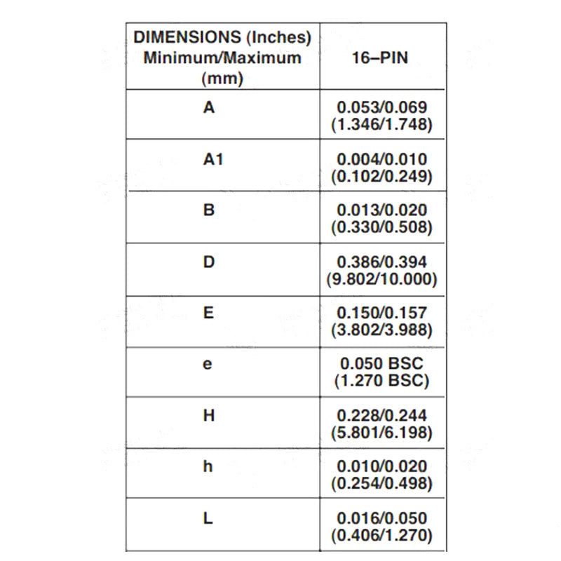
- Package: SOP-16 (SMD, 1.27mm pitch, 10mm body width)
- Supply Voltage (VCC): 8V – 35V
- UVLO Threshold: 8V turn-on / 5.6V turn-off (undervoltage lockout)
- Reference Output (VREF): 5.1V ±1%, up to 50mA load
- Oscillator Frequency: 100Hz – 500kHz (set by external RT and CT)
- Output Stage: Push-pull totem-pole, 400mA source / 400mA sink per output (OUT A and OUT B)
- Output Duty Cycle: 0–45% per output (90% total, with dead time)
- Dead Time: Programmable via RD resistor (prevents simultaneous conduction / shoot-through)
- Soft-Start: Built-in, controlled by external capacitor on SS pin (pin 8)
- Shutdown: Logic-level SD pin (pin 10, active HIGH) — latching or non-latching depending on circuit
- Error Amplifier: Internal transconductance op-amp, access to INV input (pin 1), NI input (pin 2), and COMP output (pin 9)
- Sync: Oscillator sync input (pin 3) for multi-unit synchronization
- Operating Temperature: 0°C to +70°C (SG3525A) / −40°C to +85°C (SG3525ADR)
- Quantity: 10 or 20 pieces per pack
SOP-16 Pinout
- Pin 1 — INV: Error amplifier inverting input (feedback from output voltage divider)
- Pin 2 — NI: Error amplifier non-inverting input (reference setpoint)
- Pin 3 — SYNC: Oscillator synchronization input
- Pin 4 — OSC OUT: Oscillator output (sawtooth waveform)
- Pin 5 — CT: Timing capacitor (sets oscillator frequency with RT)
- Pin 6 — RT: Timing resistor
- Pin 7 — RD: Dead time resistor (higher resistance = more dead time)
- Pin 8 — SS: Soft-start capacitor (larger cap = slower startup ramp)
- Pin 9 — COMP: Error amplifier output / compensation network node
- Pin 10 — SD: Shutdown input (HIGH = outputs disabled)
- Pin 11 — OUT A: Push-pull output A (drives high-side or primary switch A)
- Pin 12 — GND: Signal and power ground
- Pin 13 — VCC: Supply voltage (8–35V DC)
- Pin 14 — OUT B: Push-pull output B (drives low-side or primary switch B)
- Pin 15 — VREF: 5.1V precision reference output (bypass with 100nF to GND)
- Pin 16 — VC: Output stage supply (can be separate from VCC for level shifting)
Oscillator Frequency Design
The oscillator frequency is set by RT (pin 6) and CT (pin 5):
f ≈ 1 / (CT × (0.7 × RT + 3 × RD))
Typical starting values for common frequencies:
- 20kHz: RT = 22kΩ, CT = 2.2nF, RD = 200Ω
- 50kHz: RT = 10kΩ, CT = 1nF, RD = 100Ω
- 100kHz: RT = 5.6kΩ, CT = 470pF, RD = 100Ω
OUT A and OUT B switch alternately at half the oscillator frequency, each with a maximum duty cycle of ~45% (dead time fills the remaining ~10%).
Voltage Feedback Loop
Connect the output voltage divider (R1/R2) to the INV input (pin 1). Connect VREF (pin 15) through a resistor divider to the NI input (pin 2) to set the regulation setpoint. The error amplifier output (COMP, pin 9) modulates the PWM duty cycle via the internal comparator — increasing duty cycle when output voltage drops below setpoint, decreasing when above. Add a compensation network (RC) between COMP and INV for loop stability.
Soft-Start Operation
Connect a capacitor (typically 1–10µF) from SS (pin 8) to GND. At power-up, the internal current source charges this capacitor slowly, ramping the duty cycle from 0% to the steady-state value over a controlled time period — preventing inrush current and transformer saturation during startup.
Shutdown and Protection
Drive SD (pin 10) HIGH to immediately disable both outputs. Use this pin with an overcurrent comparator, OVP circuit, or microcontroller GPIO for fault protection. The SD pin can also be used for pulse-by-pulse current limiting when driven by a fast comparator monitoring primary current.
SG3525A vs. SG3524 vs. TL494
- SG3525A: Push-pull outputs (OUT A and OUT B alternate), built-in dead time, soft-start, UVLO. Best for half-bridge and push-pull topologies.
- SG3524: Older predecessor, similar architecture but lower output current (100mA) and no built-in soft-start.
- TL494: Similar voltage-mode PWM controller, two outputs, widely used in ATX power supplies. Less dead time control flexibility than SG3525A.
Typical Applications
- Half-bridge SMPS (offline AC-DC, 100W–2kW)
- Full-bridge DC-DC converter (high-power, bidirectional)
- Push-pull DC-DC converter (12V→220V inverter driver stage)
- Uninterruptible power supply (UPS) inverter PWM control
- Solar inverter PWM generation stage
- Battery charger constant-current / constant-voltage PWM controller
- Electronic ballast for fluorescent lamps
- Motor drive PWM generation (with external gate drivers)
Design Notes
- Add 100nF ceramic bypass capacitors on VCC (pin 13) and VREF (pin 15) to GND, placed as close to the IC as possible
- The SG3525A outputs (OUT A/B) can directly drive small MOSFETs at low frequencies; for higher frequencies or larger MOSFETs, add a dedicated gate driver IC (e.g., IR2104, TC4420) between the SG3525A outputs and the MOSFET gates
- Keep the RT/CT oscillator network away from switching noise sources on the PCB
- Use a ground plane and separate analog and power ground returns to minimize noise coupling into the error amplifier
Package Contents
- 10 or 20 × SG3525A / SG3525ADR SOP-16 PWM controller IC (quantity as selected)