


Keszoox
0.1mm PCB Link Wire Copper Solder | Jumper Wire for Mobile Phone & PCB Repair | Precision Rework
0.1mm PCB Link Wire Copper Solder | Jumper Wire for Mobile Phone & PCB Repair | Precision Rework

Couldn't load pickup availability
0.1mm PCB Link Wire — Copper Solder Jumper Wire for Mobile Phone & PCB Repair
The essential consumable for professional PCB rework, mobile phone board repair, and BGA reballing. 0.1mm diameter copper link wire is used to bridge broken PCB traces, bypass damaged vias, create solder bridges between pads, and repair open circuits caused by physical damage, corrosion, or manufacturing defects. At 0.1mm diameter, this wire is fine enough to route between closely-spaced SMD pads and under BGA packages without bridging adjacent conductors. The tinned copper construction solders cleanly with standard flux-core solder and flux paste, and the wire holds its shape when bent — essential for routing across component bodies and through tight spaces on densely populated boards.
Specifications
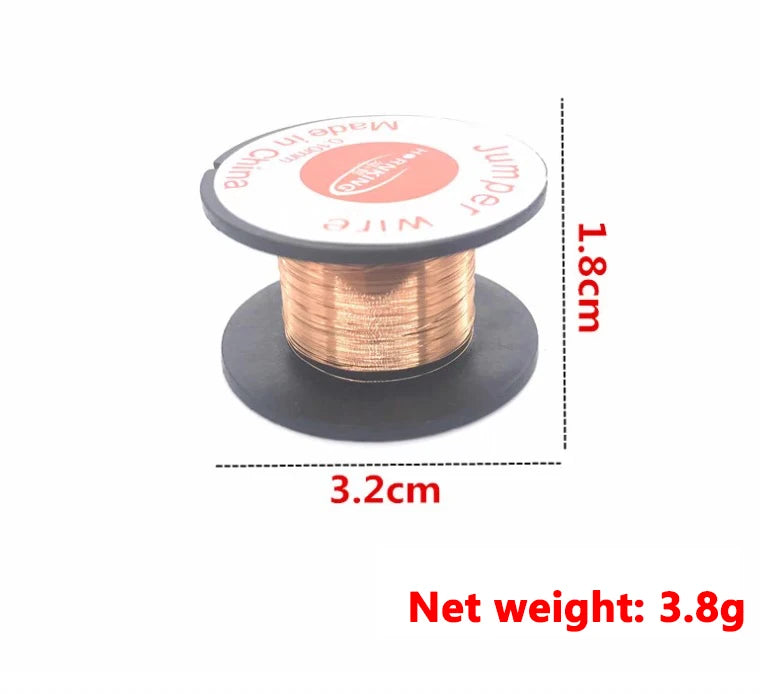
| Wire Diameter | 0.1mm |
| Material | Tinned copper (Cu) |
| Application | PCB trace repair, mobile phone board rework, BGA repair |
| Solderability | Excellent (tinned surface, compatible with standard solder and flux) |
| Condition | New |
| Origin | Mainland China |
When to Use PCB Link Wire
PCB link wire is the correct repair method when:
- Broken PCB trace — physical damage (drop, flex, impact) has cracked or severed a copper trace. Route the link wire from pad to pad, bypassing the break.
- Corroded trace — liquid damage has dissolved the copper trace. Clean the corrosion, expose the copper at each end, and bridge with link wire.
- Damaged via — a through-hole via has lost continuity. Solder link wire through the via hole or bridge the top and bottom pads.
- BGA pad repair — a BGA pad has lifted or delaminated. Route link wire from the pad to the nearest accessible point on the same net.
- Short circuit bypass — reroute a signal around a damaged section of the PCB.
- Prototype modification — add connections between pads during hardware bring-up and debugging.
Key Features
- ✅ 0.1mm diameter — fine enough to route between 0402 SMD pads and under BGA packages
- ✅ Tinned copper — excellent solderability with standard Sn63/Pb37 and lead-free solder alloys
- ✅ Shape-retaining — holds bends and routes without springing back, enabling precise placement on densely populated boards
- ✅ Low resistance — copper conductor provides negligible resistance for signal and power trace repairs
- ✅ Compatible with flux paste — use with rosin flux or no-clean flux paste for clean, reliable solder joints
Common Applications
- Smartphone and tablet PCB trace repair (water damage, drop damage)
- Laptop motherboard trace repair
- BGA reballing and pad repair
- Game console board repair (PlayStation, Xbox, Nintendo)
- Automotive ECU board repair
- Industrial PCB rework and modification
- Prototype hardware modification and debugging
- Microwave and RF PCB repair
Repair Technique Guide
- Identify the break: use a multimeter in continuity mode to locate the open circuit. Mark both ends of the break.
- Prepare the pads: use a scalpel or PCB scraper to expose clean copper at both ends of the break. Remove solder mask as needed.
- Apply flux: apply rosin or no-clean flux paste to both pads and the repair area.
- Route the wire: cut a length of 0.1mm link wire slightly longer than needed. Route it from pad to pad, bending around components as required.
- Solder: tack one end first, then route and tack the other end. Apply minimal solder — the tinned wire requires very little additional solder.
- Verify: check continuity with a multimeter. Inspect under magnification for solder bridges to adjacent pads.
- Insulate: apply UV-cure solder mask or conformal coating over the repair to protect against shorts and corrosion.
Frequently Asked Questions
Q: What soldering iron tip temperature should I use?
A: Use 300–320°C for leaded solder, 340–360°C for lead-free solder. Use a fine conical or chisel tip. Avoid excessive heat that can lift adjacent pads.
Q: Can I use this wire for power traces carrying significant current?
A: 0.1mm copper wire has a current capacity of approximately 0.1–0.2A. For power traces carrying more than 0.2A, use multiple parallel strands or a larger diameter wire.
Q: Is this wire insulated?
A: No. This is bare tinned copper wire. Route carefully to avoid contact with adjacent conductors. Apply solder mask or conformal coating after repair to insulate.
Package Contents
- 1× Reel of 0.1mm PCB Link Wire (copper, tinned)