


Keszoox
FR4 Single-Side Copper Clad PCB Laminate — 7×10cm, 1oz Copper, 1.5mm, DIY Etching
FR4 Single-Side Copper Clad PCB Laminate 7×10cm, 1oz Copper, 1.5mm, DIY Etching

Couldn't load pickup availability
FR4 Single-Side Copper Clad PCB Laminate — 7×10cm, 1oz Copper, 1.5mm, DIY Etching
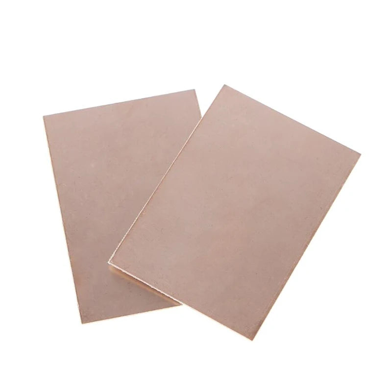
This FR4 single-side copper clad laminate (CCL) provides a blank copper-coated fiberglass substrate for DIY PCB fabrication by chemical etching, CNC milling, or laser ablation. The 1oz (35μm) copper layer on one side of the 1.5mm FR4 substrate is suitable for most low-to-medium current PCB traces. Used by electronics hobbyists, students, and engineers for prototyping custom PCBs without commercial PCB fabrication lead times.
Key Specifications
| Parameter | Value |
|---|---|
| Board Size | 7 × 10cm (70 × 100mm) |
| Substrate Material | FR4 fiberglass (UL94 V-0) |
| Board Thickness | 1.5mm |
| Copper Layer | Single-sided (one side) |
| Copper Weight | 1oz (35μm / 0.035mm) |
| Copper Purity | 99.9% electrolytic copper |
| Surface | Bare copper (no solder mask or silkscreen) |
DIY PCB Fabrication Methods
| Method | Tools Needed | Resolution | Best For |
|---|---|---|---|
| Chemical etching (toner transfer) | Laser printer, iron, FeCl3 or Na2S2O8 | ~0.5mm traces | Through-hole circuits, simple layouts |
| Chemical etching (UV photoresist) | UV lamp, photoresist film, developer | ~0.2mm traces | Fine-pitch SMD circuits |
| CNC milling (PCB router) | CNC router (Genmitsu, 3018 Pro) | ~0.3mm traces | No chemicals, fast turnaround |
| Laser ablation | CO2 or diode laser engraver | ~0.3mm traces | Quick single-layer boards |
Why Choose FR4 Copper Clad Laminate?
- FR4 substrate — superior to paper phenolic (FR1/FR2): stronger, moisture-resistant, better electrical insulation
- 1oz copper (35μm) — standard weight for most PCB designs; handles up to 1A per mm trace width
- 7×10cm size — large enough for most prototype circuits; can be cut to smaller sizes
- Bare copper surface — ready for toner transfer, photoresist, or direct CNC milling
- No lead time — fabricate your PCB in hours, not days
Compatible With / Common Use Cases
- Toner transfer etching: Print circuit on laser printer, iron onto copper, etch with FeCl3 solution
- UV photoresist etching: Apply photoresist film, expose with UV through transparency, develop and etch
- CNC PCB milling: Use 3018 Pro or Genmitsu CNC router with 0.1mm V-bit to mill traces directly
- Custom Arduino shield: Fabricate a custom shield PCB for specific sensor/actuator combinations
- RF circuit prototyping: Controlled-impedance microstrip lines for antenna and RF filter design
Frequently Asked Questions
Q: What etching chemical should I use for DIY PCB etching?
A: Two common options: (1) Ferric chloride (FeCl3) — fast, effective, but stains everything brown and requires careful disposal. (2) Ammonium persulfate (Na2S2O8) — clear solution, easier to see progress, safer disposal. Both work well with toner transfer and photoresist methods. Use at 40–50°C for faster etching.
Q: Can I cut this board to a smaller size?
A: Yes. Score with a utility knife along a straight edge and snap, or cut with a rotary tool (Dremel with fiberglass cutting disc). For clean straight cuts, use a PCB shear or guillotine cutter. Always wear a dust mask — FR4 fiberglass dust is a respiratory hazard.
Q: What is the minimum trace width I can achieve with toner transfer etching?
A: With a good laser printer (600 DPI minimum, 1200 DPI preferred) and careful ironing technique, traces as narrow as 0.5mm (20 mil) are reliably achievable. Traces below 0.3mm require UV photoresist or CNC milling for consistent results.
Package Contents
- 1× FR4 Single-Side Copper Clad PCB Laminate (7×10cm, 1oz copper, 1.5mm)