- ★Product Description
- ★About us
- ★Custom cable
Converts between 3.3V and 5V using SN74LVC4245A octal transceiver
DESCRIPTION
The Hi-Speed 8-Channel Logic Level Converter Module utilize the SN74LVC4245A octal bus transceiver to convert logic levels up or down anywhere between 3.3V and 5V at full logic speeds.
PACKAGE INCLUDES:
- Hi-Speed 8-Ch Logic Level Converter Module
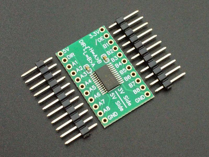
- Qty 2 -11-pin male header strips, optionally soldered on
KEY FEATURES OF HI-SPEED 8-CHANNEL LOGIC LEVEL CONVERTER MODULE:
- 8 Channels with direction control and output enable
- Convert logic levels Up or Down between 3.3V and 5V systems
- Operates over full speed range up to 70MHz
- Strong 24mA drive current capability
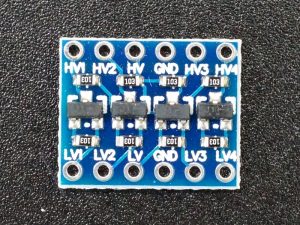
MOSFET Level Converter
The vast majority of logic level shifters on the market utilize MOSFET transistors for the conversion process. These work great for relatively slow speed signals of under 1Mhz, especially when the signals need to be bi-directional such as with I2C. We sell these ourselves. Unfortunately, when these MOSFET modules are used for high speed logic conversion, their speed limitations often prevent them from working at all, or worse they create intermittent data that can be hard to diagnose.
This module on the other hand is specifically designed for handling the full range of parallel data bus speeds up to 70MHz. All data lines on the module are routed straight across the module with no vias and the chip has bypass caps on all power pins to optimize performance. Any performance limitation will typically be due to the breadboard wiring used.
Module Operation
This module is typically used to connect 3.3V and 5V parallel data buses together such as for driving a 5V 8-bit parallel display interface from a 3.3V MCU or vice versa. It can also be used for converting individual data lines.
The data lines are directional so cannot be used for bi-directional data lines such as used with I2C.
Power
There are two power pins on the module.
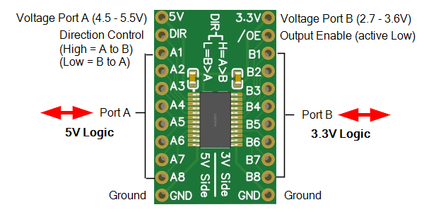
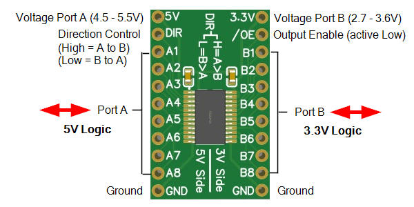
5V pin connects to 4.5-5.5V (5V typical) and powers the Port A side of the device.
3.3V pin connects to 2.7-3.6V (3.3V typical) and powers the Port B side of the device.
There are two GND pins of which only one needs to be connected to ground as the pins are connected together on the module. If the 5V and 3.3V power systems are separate without a common ground, then both should be connected to the ground pins.
Direction Control
The DIR (Direction Control) pin is an input that determines which direction the data flows, either from Port A to Port B or from Port B to Port A.
If the DIR pin is pulled HIGH, the data flows from Port A to Port B. If it is pulled LOW, the data flows from Port B to Port A. This pin should not be left floating or erratic operation can result.
If the data will always flow in the same direction, this pin can be simply hardwired to 5V/3.3V or ground to set the desired direction. It can also be controlled by a microcontroller. The input is both 3.3V and 5V logic compatible.
Output Enable
The /OE pin is an input that controls whether the outputs are driven (enabled) or tri-stated (disabled).
A logic LOW enables the outputs. If the outputs will always be enabled, this pin can simply be hardwired to ground. This pin can also be controlled by a microcontroller and the input is both 3.3V and 5V logic compatible.
Logic control of this pin is usually done if the outputs are driving a bus that may also be driven by other chips at times. The microcontroller can use the /OE pins of the deivces to determine which device has control of the bus at a given time. It can also be used to prevent driving signals into a device that is unpowered to avoid possible damage.
Module Connections
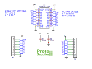
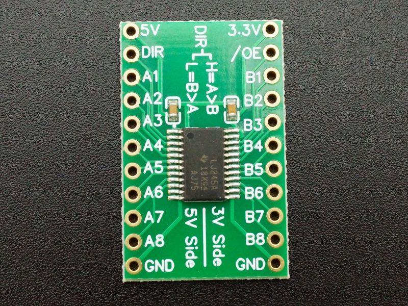
The module is laid out so that the Port A (5V) is on the left and Port B (3.3V) is on the right side of the module. Note that although the SN74LVC4245A chip has 24-pins, this module has 22 pins. A 3rd redundant ground and an extra 3.3V pin have been removed and the Port A and Port B pins have been lined up to be straight across from each other for easier wiring.
The board has the following connections:
- 5V = Port A power (4.5 – 5.5V)
- 3.3V = Port B power (2.7-3.6V)
- DIR = Direction Control. Logic H = Port A to Port B, Logic L – Port B to Port A
- /OE = Output Enable. Logic L = outputs enabled. Logic H = outputs tristated.
- GND = Ground. Should be common to both voltage systems. Only one ground pin needs to be connected
- A1-A8 = Port A data lines
- B1-B8 = Port B data lines
ASSEMBLING THE MODULE
The module comes with 2 strips of straight male headers. These can be soldered on for use with a breadboard, or you can use right-angle headers or attach wires directly to the board depending on what your application requires.
To ensure good alignment during soldering first insert the loose headers into a solderless breadboard. The board can then be placed on top of the headers and easily soldered in place.
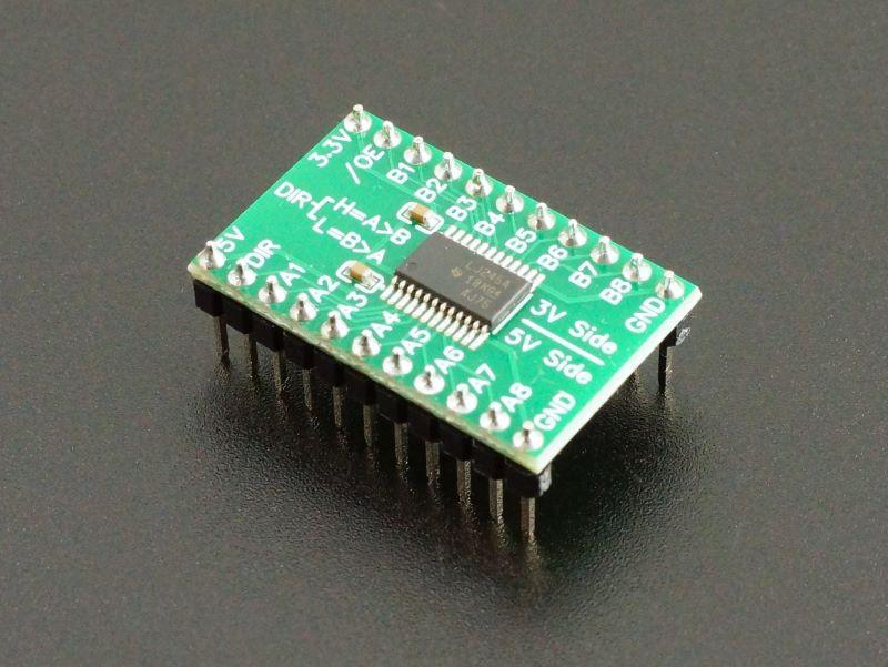
The module can also be ordered with these pins already soldered on for plug-n-play operation.
BEFORE THEY ARE SHIPPED, THESE MODULES ARE:
- Sample tested per incoming production build.
Notes:
- None
TECHNICAL SPECIFICATIONS
| Operational Ratings | ||
| 5V | Voltage Port A | 4.5V – 5.5V (5V typical) |
| 3.3V | Voltage Port B | 2.7 – 3.6V (3.3V typical) |
| Maximum Chip Data Rates | 70MHz | |
| Dimensions | L x W (PCB) | 27.9x 17.78mm (1.1″ x 0.7″) |
| Footprint | DIP-22 on 0.6″ centers | |
| Country of Origin | Designed in USA | Manufactured in China |
| Datasheet | Texas Instruments | SN74LVC4245A |


